What is pcb?

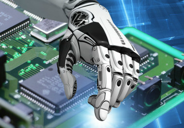
The full name of PCB is printed circuit board. It is an important electronic component and the carrier of electrical connection of electronic components. The electronic products used in our lives all contain printed circuit boards. Because it is made of electronic printing, it is called a "printed" circuit board. Next, FS Tech will introduce you to the relevant knowledge of pbc.
The birth of PCB
The creator of the printed circuit board was the Austrian Paul Eisler. In 1936, he used printed circuit boards for the first time in the radio. After seeing the convenience and benefits of pcb, people at that time began to develop the printed circuit board industry slowly, and then pcb became more and more common in life. China is still in pcb. During the development period of , its technology is not very mature, of course, there is also a leader in the pcb industry - FS technology. In 1943, printed circuit board technology was widely used in military radios in the United States, because their military value is very detailed, one is because a small pcb board can carry a lot of information, and the other is because of its small size, it is very suitable for the military field. . In 1948, the United States began to give pcb commercial value, which is why pcb is now used in our lives. Printed circuit boards have been extensively developed since the mid-1950s. FSPCBA saw the development prospects of PCB, so it has been engaged in the PCB industry since 2010. As a veteran PCB assembly and manufacturer in China, it has always been in a leading position in the industry.

The dominance of pcb in electronics manufacturing
Before the advent of the PCB, the interconnection between electronic components was done through the direct connection of wires. Today, pcb boards replace wires and are used in all electronics manufacturing, while wires are buried in laboratories; printed circuit boards (PCBs) undoubtedly occupy an absolute control position in the electronics industry.
With the passage of time and the advancement of technology, the circuit board industry has gradually developed. Printed boards have evolved from single-layer to double-sided, multi-layer and flexible, and are still holding their own. It is worth mentioning that the best printed circuit board company in the world is still in the United States, while the best printed circuit board company in China can only produce a hundred layers of circuit boards. With the continuous development of high precision, high density and high reliability, as well as the continuous reduction of volume, cost and performance. The printed circuit boards of FS Tech are gradually showing their edge. I believe that FS Tech will still maintain strong vitality in future electronic equipment development projects.
How the circuit board works
The working principle of the printed circuit board is actually not difficult. It uses the insulating material of the board to isolate the conductive layer of the surface copper foil, so that the current flows in each element along the pre-designed route, so as to complete the functions of work, amplification, attenuation, modulation, demodulation, coding and so on.

FS Tech often concentrates parts on one side and wires on the other side when manufacturing the most basic PCBs. Because the wires only appear on one side, we call this type of board a single-sided pcb. The multi-layer board process is what all circuit board companies are pursuing. The more layers of the board, the stronger the company's strength. FS Tech can only produce 25-layer hard brushed circuit boards. Multi-layer boards, as the name suggests, have multiple layers. A pcb of wires, there must be a proper circuit connection between the two layers. The bridges between circuits are called vias. The basic design process of a circuit board can be divided into the following four steps:
- Circuit schematic design---circuit schematic design mainly uses the schematic editor of Protel DXP to draw the schematic diagram.
- Generate a network report - a network report is a report that shows the circuit principle and the relationship between the various components in it. It is a bridge and link connecting circuit schematic design and circuit board design. Through the network report of the circuit schematic diagram, the connection between the components can be quickly found, thus facilitating the subsequent PCB design.
- Design of printed circuit board---The design of printed circuit board is what we usually call PCB design. It is the final form converted from the circuit schematic. This part of the relevant design is larger than the design of the circuit schematic. We can use the powerful design function of Protel DXP to complete this part of the design.
- Generate printed circuit board report --- After the printed circuit board design is completed, various reports need to be generated, such as generating pin report, circuit board information report, network status report, etc., and finally print out the printed circuit diagram.


